OVERVIEW
Today’s semiconductor industry faces a dynamic nature in either SOC or SiP path-finding and diversity of applications in IoT, automotive, mobile, high-performance computing and even heterogeneous components integration. For example, a top-level layout assembly task normally manages hundreds of sub-blocks in either a SOC GPU chip, or an advanced-node testchip design, or a multi-chip SiP project; while each sub-block owner may have many design re-spins. A high-performance layout integration platform is highly desired to embrace the common challenges in chip-scale, wafer-/panel-level layout integration of complicated design intents, post ECO & dummy engineering, revisions and huge data size and/or with multiple database formats.
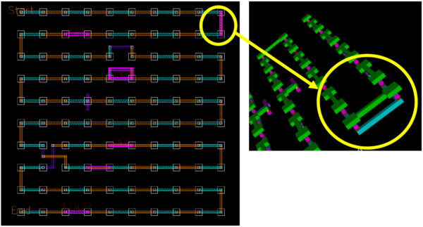
THUNDER is a versatile layout integration platform to support heavy layout handling efforts from post P&R, IP merge automation & management, physical ECO verification (XOR LVL, connectivity, etc.), DRC/LVS debugging interface, and even (in-line inspection) defect-to-layout mapping, failure analysis and chip-package integration (fanout, interposer and substrate routing, pins connectivity, etc.).
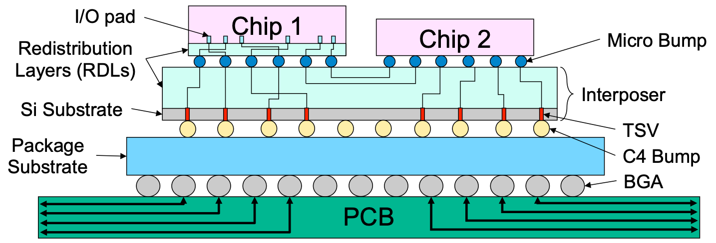
As technology advances, interposer-based three-dimensional integrated circuits (interposer-based 3D ICs, or known as 2.5D ICs) become one of the most promising solutions for enhancing system performance, decreasing power consumption, and supporting heterogeneous integration. The 2.5D IC packaging is a technique for connecting multiple dice to an external circuitry such as package substrates. To ease design changes, a silicon interposer is introduced as an interface between chips and a package. Multiple chips can be mounted on the interposer, and inter-chip nets are routed on the redistribution layers (RDLs) of the interposer by chip-scale wires.
MAJOR FEATURES
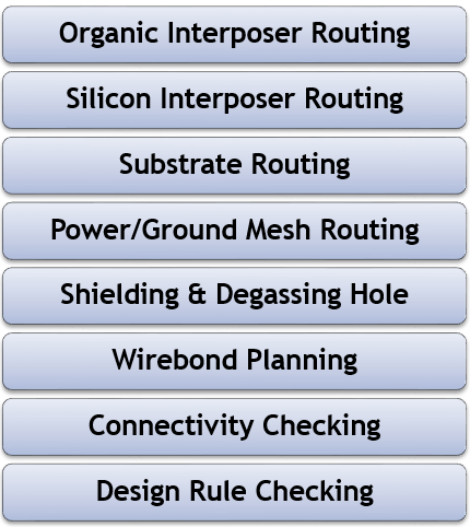
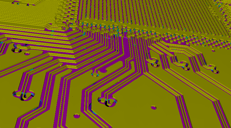
Organic Interposer Routing
- Octilinear compact routing style
- Staggered/stack via
- Huge capacity for big die package design
- Efficient performance
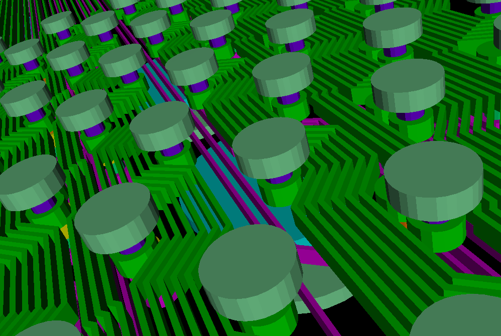 Silicon Interposer Routing
- Micro bump to micro bump routing
- Micro bump to bump routing
- Redundant via
- Staggered/stack via
- TSV creation
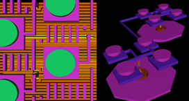
Substrate Routing
- Net priority: high-speed net, differential pair
- Net grouping
- Length-matching routing for grouped nets
- Mixed any angle/octilinear routing
- Mixed minimum/variable net width/spacing
- Via location constraint vs. critical net
- Redundant via
- Stack/offset via
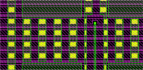
Power/Ground Mesh Routing
- Parallel metal lines for power/ground
- Add via to crossing area
- Support orthogonal/diagonal modes
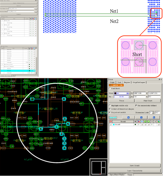
Connectivity Checking
- Check interconnections of multiple chips
- Highlight open/short locations
- Support multiple input formats of netlist
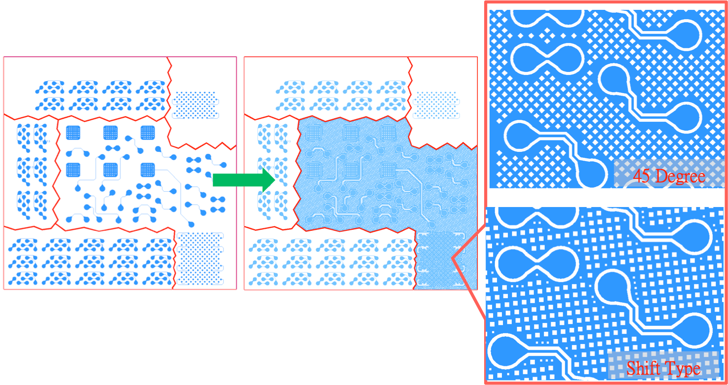
Shielding & Degassing Hole
- Area fill for multiple P/G domains
- Flexible filling/hole constraints customization
- Multiple hole types
- Diagonal hole
- Density prediction
- Dummy insertion by specified density
- Ground Net trace and merge
- Huge capability and high performance
Design Rule Checking
- Supported rules: Spacing, Width, Enclosure, Inside, Outside, Angle
- Support TCL/PERL to integrate rule combinations

Wirebond Planning
- Interactive interface for modifying the wire bonding
- Multi-die (MCM) supported
- LVS (Open/Short) check
- Output the bonding table and diagram for the packaging house

Daisy Chain Creation & Checking
- Daisy chain ordering
- Daisy chain open/short checking
- Create daisy chain with bump file